


In an interview with Bit-tech GlobalFoundries has discussed its plans for the future and talked up its 28nm manufacturing process that is substantially different from competing nodes at TSMC and Samsung. Besides that it tells the story of 20nm and 14nm, and talk about the possibilities and difficulties of these nodes.
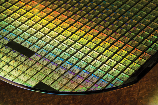
Large portions of the semiconductor industry is ready to move on to 28nm and for the first time TSMC have real competition from two other companies. Besides Samsung that has entered the game we also have GlobalFoundries, and the latter has a secret ingredient to make it stand out.
As earlier reports have stated GlobalFoundries uses a gate-first method, unlike others in the industry that chooses to go gå Gate-last. The big advantage of Gate-first is that it saves 10-20% circuit spave at 28nm over gate-last. The difference between Gate-first and Gate-last is when you add the transistor ports to a wafer.
Most have swapped the silicon-based components to Metal Gate and High-K isolators made from more exotic materials like Hafnium, often called HKMG. Gate-first is different in the way that these components are installed on a production wafer before it is time to heat things up.
The disadvantage with Gate-first is overall lower yields, less working chips per wafer. When GlobalFoundries gets a question about this it replies that Gate-first is the right alternative for GlobalFoundries, and there are currently no problems. The saved space will offer a superior value over Gate-last.
Even though it is boasting its gate-first production Dirk Wristers says the 20nm node will use Gate-last just like Intel and TSMC. Its 20nm process will shrink the circuit surface with 50% from 28nm and he says that GF had to be really innovative here. Density and scaling advantages of gate-first HKMG doesn’t apply because of pattern dominated liography limitations. It expects to have the 20nm process ready in 2013, most likely by the end of that year, and we doubt there will be any products on the market until 2014.
 Illustrative picture, 32nm planar-transistor (left), 22nm Tri-gate transistor (right).
They also talked about Intel’s coming 3D transistor at 22nm, or Tri-gate transistor. it confirmed GF is doing 3D activity and earlier have mentioned some form of Multigate transistor at 14nm. What this means is that it can close the electron flow much more efficiently to lower leakage. It has not decided what it will base the 14nm process on, but it will definitely be something in line with what Intel will bring next year.
On the mobile side with ARM-based circuits at 28nm it looks like TSMC has collected the most customers, but also Samsung and GlobalFoundries are expected to grab a share of the market. When it comes to graphics cards NVIDIA is expected to continue at TSMC, while unconfirmed rumors implies AMD will split its manufacturing of GPU between TSMC and GlobalFoundries. One partner will make VLIW-4 based GPUs, while the second will make the high-end circuits based on AMD’s fresh architecture.
One thing is for certain, many are uncertain if GlobalFoundries can deliver, especially since it is working on a, according to them, superior 28nm process. The execution of 28nm will be brand it for many years to come.
Source: Bit-tech
Relaterade nyheter:


Leave a Reply