


We look forward to the launch of AMD Trinity this Summer, but have already acquired some new information on the successor. Besides the third generation Bulldozer architeture it will sport a graphics processor on the level with the just launched HD 7700 series.
We know that AMD is planning to launch the third generation APU in 2013, Kaveri – a processor with integrated graphics, and once again it will raise the bar for such a circuit. Kaveri will be the first product from the company that will make the memory non-exclusive, that is processor and graphics circuit will be able to share the memory. No matter if it is graphics built into the motherboard or the processor, the graphics processor has had to allocate a certain amount in the past. In practice it means that all RAM will then be available to both processor and graphics circuit.
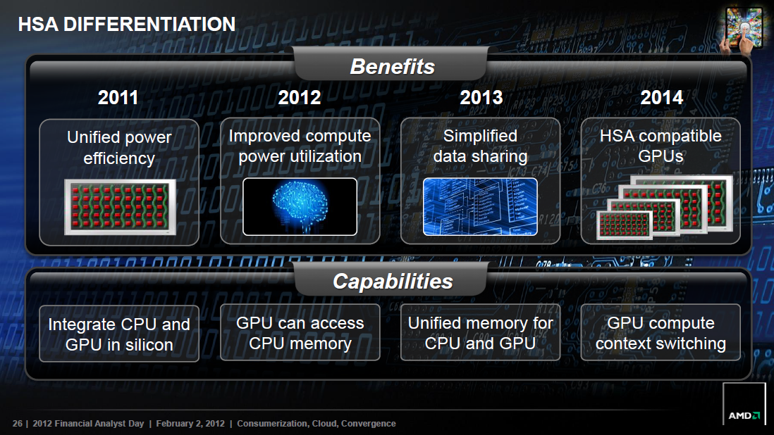
Documents from AMD have revealed specifications for Kaveri, which at first sight reminds us of a recently launched circuit. Besides third generation Bulldozer architecture ”Steamroller”, it will get 8 GCN units, which is the exact same as Radeon HD 7750. There is talk that Kaveri will go up to 100W just like the precursor, and be the first APU to reach 1 TFLOPS (Tera Floating-Point Operations Per Second).
| Architecture | Kaveri ”2013” | Trinity ”2012” | Llano ”2011” |
| Node | 28nm | 32nm | 32nm |
| Processor architecture |
Steamroller | Piledriver | Husky |
| Processor cores |
4 | 4 | 4 |
| Processor frequency |
~4 GHz(?) | ~4 GHz | ~3 GHz |
| L2 cache | 2 x 2 MB(?) | 2 x 2 MB | 4 x 1 MB |
| Memory channels |
? | 2, 128-bit | 2, 128-bit |
| Graphics architecture |
GCN | VLIW4 | VLIW5 |
| Clusters GCN/VLIW | 8 | 6 | 5 |
| Radeon-kärnor | 512 | 384 | 400 |
| Graphics frequency |
900 MHz(?) | 800 MHz | 600 MHz |
| Texture units |
32 | 24 | 20 |
| ROPs | 16 | 8(?) | 8 |
| Video decoder |
? | VCE/UVD3 | UVD3 |
| TDP | 100W | 100W | 100W |
| Performance (GFLOPS) | 1 050 | 819 | 573 |
| Socket | ? | FM2 | FM1 |
The graphics will be upgraded big time since it at least on paper will equal Radeon HD 7750. If Kaveri gets dual-channel memory we can imagine that memory bandwidth can be limiting in games through. But since the APU will be able to handle the memory in a whole new way it possible this will not be as much of a problem as it is with Llano. We don’t know which socket it will use, and if it decides to move over to more memory channels it would definitely help. This is unlikely though since APUs in general are meant to be affordable and another memory channel will add considerable cost to the platform.
 Performance on par with HD 7750 – but what about the memory?
Kaveri has performance over 1 TFLOPS, or more precise 1050 GFLOPS, which gives us a hint of the clock frequencies it will use. If the processor gets four cores at 4 GHz, it will contribute with 128 GFLOPS, which means the GPU will contribute the most. Radeon HD 7750 with its 512 Radeon cores is currently at 819 GFLOPS with a clock frequency at 800 MHz. Kaveri would need a graphics circuit at 900 MHz and 921.6 GFLOPS to reach 1049.6 GFLOPS.
The 28nm manufacturing technology is expected to a half-node of GlobalFoundries’ 32nm SOI/HKMG technology that AMD uses today. Even if the move to 28nm may sounds minor it will bring a boost in transistor density by 25 percent. If AMD can keep its 1 year schedule on the APU front Kaveri should arrive for the Summer 2013. Intel will have had processors at 22 nm for over a year by then, and Kaveri will be going up against the next generation Haswell.


Leave a Reply