

NVIDIA revealed details on the next generation graphics circuit architecture. Code-named Fermi the architectures promises to change our view on the modern GPU, but w’re wondering what it means to GeForce and games overall.
NVIDIA is somewhere between a rock and AMD, as the latter has already announced its new generation of graphics circuits with DirectX 11 support and impressive performance, resulting showers of praise from reviewers. NVIDIA can’t possibly sell any graphics cards based on the new architecture and it might take even until next year before we can witness the first DirectX 11 graphics cards from NVIDIA in noticeable quantities.
NVIDIA has to do something and fast to not lose the support from partners and consumers, which resulted in a somewhat unusual announcement of its new graphics circuit architecture Fermi earlier this week. NVIDIA’s bew GPU archicture has been dubbed Fermi after the Italian physicist and contributor to the development of the atomic bomb, and to be completely honest we can’t quite put our finger on why it went with this name. With more than 3 billion transistors Fermi is the GPU equivalent to a nuclear reactor, while at the same time NVIDIA is working hard on luring scientists and companies worldwide to use its new GPU architecture.
If we just accept that the graphics processor has been named Fermi we can return to NVIDIA’s new architecture and try to figure out why it is so far behind AMD in the development. The biggest reason is the mere size of it, with TSMC’s new 40nm manufacturing process NVIDIA has loosened the ties a bit and added a lot more transistors and when we thought Radeon HD 5870 was big with 2.15 billion transistors it becomes close to ridiculous when NVIDIA has managed to fit 3 billion inside Fermi.
|
|
GT200b
(GeForce GTX 285) |
RV870/Cypress
(Radeon HD 5870) |
GT300/Fermi
|
| Manufacturing node | 55nm | 40nm | 40nm |
| Core size | 470 mm2 | 334 mm2 | ~467 mm2* |
| Transistors | 1 400 million | 2 150 million | 3 000 million |
*Estimated
Making a graphics circuit with over 3 billion transistors takes time, it doesn’t go any faster when it at the same time restructures the GPU architecture compared to earlier generations. While AMD focuses on games and 3D performance with its Radeon HD 5000 series NVIDIA has greater plans, its words, for the Fermi architecture. Before we move on to discuss these we will look at the actual GPU and what has changed since previous generations.
NVIDIA claims that Fermi brings the biggest changes in graphics circuit development since the launch of G80 and it made comparisons to both of the previous architectures, GT200 and G80, early in the presentation. With GT200 NVIDIA raised the bar quite a bit for the number of transistors in a GPU and as you saw on the previous page Fermi will be one big chip, but thanks to the efficient 40nm technology there is little of chance of making the same mistake it did with the first GT200 GPU, GeForce GTX 280. This 65nm circuit was too big and too power consuming, but with Fermi NVIDIA hopes to have found a good balance between the transistor count and manufacturing technology.
But what does the extra 1.6 billion transistors brings? Let’s compare Fermi to NVIDIA’s previous architectures.
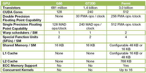
First of all, NVIDIA has more than doubled the number of shader processors, from now on called CUDA Cores. From 240 with GT200 to 512 with Fermi. NVIDIA has also made several changes in the architecture and even if the founding blocks are the same as GT200 there is much that is new.
The Fermi GPU architecture with 16 streaming multiprocessors housing 32 CUDA cores each. The green fields are CUDA cores, the light blue are registers and L1 cache.
The increased number of CUDA cores aside we can see that the floating point calculation capacity have been improved, which is the very foundation of GPGPU. At the same time NVIDIA has expanded the shared memory of the circuit and there both L1 and L2 cache integrated into Fermi. Caches are otherwise more commonly found inside our regular processors, CPUs, but it is just another hint of where NVIDIA are planning to take things.
NVIDIA has made changes to the SM architecture and this is where you find the biggest increase in floating point performance. This has been achieved by equipping the SM units with cache and adding IEEE 754-2008 support to the floating point unit. The result is a more efficient handling of 64-bit floating point calculations and much better performance in double precision.
AMD bragged about how Radeon HD 5870 offered 544 GFLOPS in double precision, many times better than the 78 GFLOPS of NVIDIA’s GT200 architecture. Through these optimizations in Fermi NVIDIA has multiplied floating point performance and the numbers shown earlier this week state that Fermi could offer around 750 GFLOPS in double precision operations. This is if NVIDIA can keep the clock frequencies of the CUDA cores in the same range as with the GT200 architecture. The exact performance hasn’t been set yet, which is mainly because the clock frequencies of the circuit hasn’t been decided yet, but either way there will be floating point performance to go around.
With all of the power available with Fermi it is vital to make sure there is enough memory bandwidth. NVIDIA knows this of course and have made multiple changes to the memory controller and the biggest is the support for the latest memory standard GDDR5. Fermi sports six GDDR5 memory controllers that unlike previous generations also support 64-bits addressing. This means that Fermi graphics cards can be equipped with over 4GB memory and we already hear of cards sporting 6GB memory buffer. This is not something that will be used in games but mainly with HPC (High Performance Computing) markets.
Fermi sports the odd 384-bit memory bus, narrower than the 512-bit bus used by GT200, but with considerably faster GDDR5 memory the total memory bandwidth will still be much higher. How much higher remains to be seen since NVIDIA hasn’t revealed the clock frequencies of the GDDR5 memory chips yet.
NVIDIA has added support for Error-Checking and Correction (ECC) in the memory controller, which means that it can, just like AMD, make sure there are no broken data in the memory. Unlike AMD’s implementation NVIDIA’s solution can also correct possible errors, which once again is very important for HPC use.
NVIDIA focusing more and more on non-graphics applications
The entire Fermi architecture emits vibes of NVIDIA’s plans to move toward applications that are not really graphics and it calls this the world’s first cGPU, computing Graphics Processing Unit. Beside tailoring the hardware toward more applications than just 3D graphics NVIDIA has also made sure Fermi ships with proper software support. Fermi takes the programming tool CUDA to a whole new level, but there is also added support for more programming languages, including C++ and Fortran.
To make it easier for developers it has developed a platform called Nexus. It runs through Microsoft Visual Studio and can come in contact directly with the hardware for troubleshooting, analyzing performance develop source code for non-graphic applications on NVIDIA’s GPUs.

NVIDIA Nexus developer platform
To sum up NVIDIA’s announcement of the Fermi architecture there is no doubt in our minds that it is feeling the heat from AMD and its recently launched GPU architecture Cypress. AMD has a powerful GPU that supports the new generation game effects through DirectX 11 and even more important is that there are more cards coming very soon.
We haven’t mentioned DirectX 11 and games much in this short introduction to the Fermi architecture and the reason is quite simple, NVIDIA barely mentioned it. It feels like a given that Fermi will perform well in games with DirectX 11, 3 billion transistors and more than twice as many CUDA cores as before. NVIDIA didn’t want to talk performance numbers at this time, and that is the biggest problem right now, time.
NVIDIA revealed quite a bit of details surrounding the Fermi architecture, but the final launch will not happen for months, if we’re lucky it will be this year. But then it will be a paper launch since we don’t expect any substantial amounts of Fermi on the store shelves until before year. If that’s the scenario we are approaching NVIDIA needs to have something truly great coming, and not just the flagship product but also products to compete in the lower price regions.

When will see this card in stores?
NVIDIA much rather talked about how Fermi will change the way we use a GPU and there is no doubt that it is opening new doors for software developers working with non-graphics applications. NVIDIA doesn’t have a CPU line-up to fall back upon and with Fermi it hopes to grab a share of the CPU industry with its coming assortment of GPUs. NVIDIA Tesla will be upgraded big time with Fermi and already the new architecture has attracted interest from supercomputer companies where they hope to use GPU-based supercomputers to increase performance exponentially.
NVIDIA has an advanced and powerful architecture with Fermi, but we’re wondering when we will actually see it and what the competition will be like when it arrives. NVIDIA will most likely be pulverized in the Holiday shoppings and if it doesn’t get the needed support for the Tesla market it is in even bigger trouble.


