


Following Intel’s investment in ASML, ASML has sent out investment proposals to other major actors on the market to collect more money to accelerate the development of future manufacturing tools. TSMC confirms that it has received the proposal, but will wait for Samsung to make a move.
ASML is leading the development of litographics tools, which the entire semiconductor industry is depdendent on to continue shrink circuits to new levels. To accelerate the development Intel has acquired 15 percent of the company for 2.55 billion euro, and invest another 830 million euro in the development of EUV litography and 450mm wafers. The move to 450 millimeter wafers from 300, is expected to lower production costs with 30 – 40 percent, while EUV can eliminate several steps in the process to further reduce costs.

ASML söker nu fler investerare och TSMC har bekräftat att de har fått ett investeringsförslag. TSMC ska enligt källor till DigiTimes vara vaksamma i väntan på om Samsung väljer att investera i bolaget. Samsung har traditionellt sett alltid givit aktivt stöd till utvecklare av litografiverktyg inom Sydkorea, men då dessa börjar halka efter är det möjligt att Samsung nappar på ASML:s förslag. Det är inte fel att anta att UMC, GlobalFoundries och övriga företag inom branschen fått samma förslag av ASML.
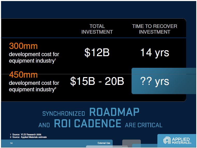
In 2000 the transition from 200 to 300 millimeter wafers resulted in the same price reduction as 450 is expected to give, but the initial investment in the development was 12 billion dollar for the industry as a whole, an investment that will have paid off until 2014 – 14 years later! For 450 millimeter the investment will be even higher with a tab of 15 – 20 billion dollar and here it is too early to speculate when the new wafer size will pay off. When it comes to these kind of sums it is not surprising that ASML is looking for other actors to help them financially in the long run.
Source: chipworks


Leave a Reply